
When you open a thyristor datasheet, the first two numbers that catch your eye are usually 8A RMS on-state current and 800V repetitive peak off-state voltage. ForS6008L, these two nominal values determine its basic application range in medium- and low-power AC switching scenarios—such as AC dimming, motor speed control, solid-state relays, and heating control. But what do "8A/800V" in the datasheet really mean in practical engineering? Which parameters decide whether it can operate stably in your circuit? This article will break down thisdatasheetitem by item, covering absolute maximum ratings, static and dynamic characteristics, triggering conditions, typical applications, and design pitfalls.
I. What is S6008L: Device Positioning and Quick Overview of the Datasheet
1.1 Product Positioning and Package Type
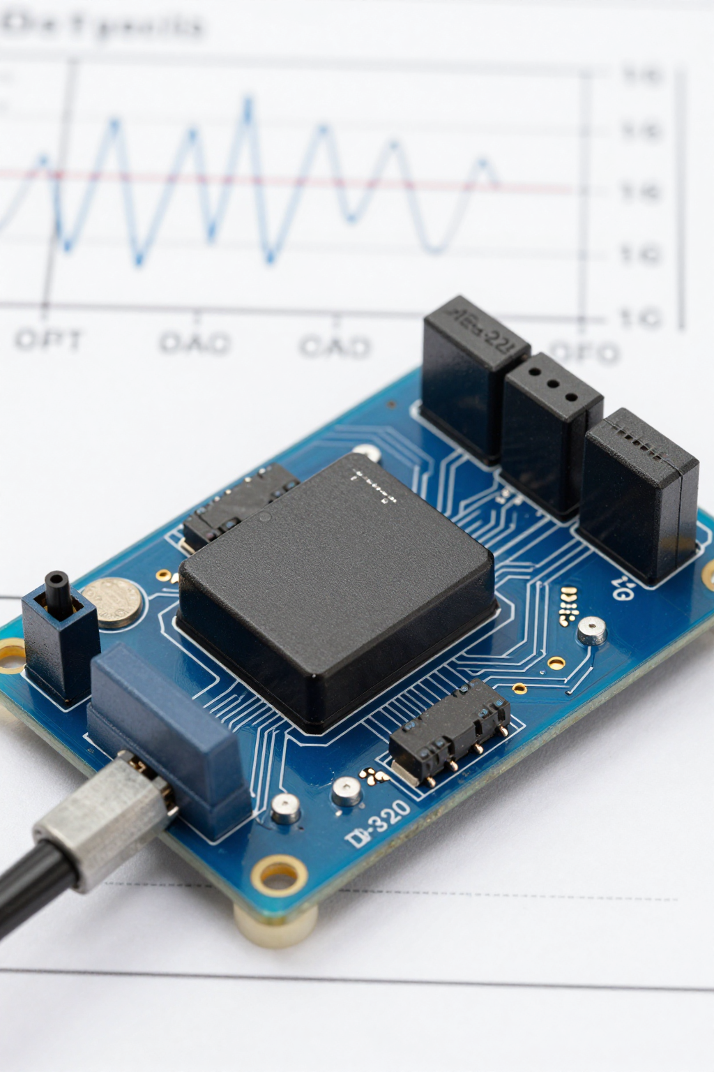
S6008LIt belongs to the unidirectional silicon controlled rectifier (SCR), not the bidirectional triac. This is the first and most easily confused distinction when selecting components: an SCR conducts only in one direction, making it suitable for DC or pulsating DC after half-wave rectification; if you need full-wave AC control, you must connect two SCRs in anti-parallel or switch to a triac.S6008LThe common package is TO-220, with pin definitions of cathode (K), anode (A), and gate (G). Heat dissipation is conducted through the metal backplane to an external heat sink.
The model naming convention on the first page of the datasheet is worth careful study: the S series denotes low-power SCRs; in "6008," "60" indicates the voltage rating, "08" corresponds to an 8 A on-state current, and the suffix "L" typically marks different trigger current levels. Compliance certifications (such as UL and RoHS) are usually listed in the footer of the first page and represent mandatory requirements for market access.
1.2 Reading Logic of the Datasheet
Efficient ReadingParametersThe order of the manual should be: Absolute Maximum Ratings → Thermal Characteristics → Static Parameters → Dynamic Parameters → Trigger Characteristics → Application Curves. First look at the limits, then at the typical values, and finally at the curves—this methodology can help you determine within ten minutes whether a device fits into your design window. Absolute Maximum Ratings tell you "what must not be exceeded," thermal characteristics tell you "how long it can withstand," static and dynamic parameters tell you "how it actually performs," and trigger characteristics decide "whether it can reliably turn on."
II. In-depth Interpretation of Absolute Maximum Ratings: The True Meaning of 8A/800V
| Parameter Name | Symbol | Value | Test Conditions |
|---|---|---|---|
| Off-State Repetitive Peak Voltage | VDRM | 800 V | Tj=25°C, Gate Open |
| Reverse Repetitive Peak Voltage | VRRM | 800 V | Tj=25°C |
| On-State Root Mean Square Current | IT(RMS) | 8 A | Tc=85°C, 50Hz Sine |
| Non-repetitive peak surge current | ITSM | 80 A | t=10ms, Half-Sine |
2.1 Current parameters: 8A is not "just running 8A"
IT(RMS)=8A is the maximum RMS current under conduction conditions, but this figure comes with strict prerequisites: the case temperature is typically constrained to a specific value (e.g., Tc=85°C or 100°C). If thermal management is inadequate, the actual usable current will drop rapidly along the derating curve. Taking ITSM (surge current) as an example,S6008LUnder a single half-sine wave, surge withstand capability can reach several tens of amperes, but the duration is limited to only half a power-frequency cycle; the I²t value quantifies the ability to handle surge energy and serves as the basis for selecting fuses and protective circuits.
More critically, there's the derating curve: in the datasheet, the IT(RMS) versus case temperature curve drops in discrete steps—each increase in case temperature results in a significant reduction in the allowable current. This means that in enclosed enclosures or without a heatsink, an 8A nominal rating may be reduced to only 3–4A. The relationship between on-state current and case/junction temperature derating is fundamentally determined by the balance between thermal resistance and power dissipation—this is why thermal design isn't an "add-on," but rather the starting point for component selection.
2.2 Voltage Parameters: Margin Design for 800V VDRM/VRRM
VDRM/VRRM=800V is the repetitive peak off-state voltage, with test conditions typically specifying junction temperature and gate bias state. In a 220V mains scenario, the peak voltage is approximately 311V, and the 800V rating provides about 2.5 times margin; in a 380V three-phase scenario, the line-to-line peak voltage is around 537V, reducing the margin to roughly 1.5 times. Engineering practice recommends maintaining at least 1.5 to 2 times voltage margin to absorb grid surges and commutation overvoltages.
It is worth noting that transient overvoltage and dv/dt are interrelated risks: rapidly rising voltages may couple through junction capacitance to the gate, causing false triggering. The dv/dt ratings listed in datasheets serve as quantitative constraints on this risk, which will be discussed further below.
III. Detailed Breakdown of Key Static and Dynamic Parameters
3.1 On-State Voltage Drop VTM and On-State Current ITM
VTM is the peak on-state voltage drop under specified gate current and junction temperature conditions, with a typical value of approximately 1.5–1.7 V. This figure directly determines the on-state power loss: P = VTM × IT(AV). Assuming an average current of 5 A, the power loss per device is roughly 7.5–8.5 W, which must be dissipated by a heat sink. The test conditions for VTM—such as gate drive current magnitude and junction temperature—can significantly affect the measured value: VTM tends to be higher when gate overdrive is insufficient, while it decreases slightly as junction temperature rises. Therefore, power loss estimates should be based on VTM values under your actual operating conditions, rather than the typical values listed on the product page.
3.2 Gate Trigger Parameters: VGT, IGT, and Latching/Holding Current
VGT and IGT represent the gate turn-on voltage and current, respectively, both of which vary with temperature: at low temperatures, the turn-on voltage increases and the turn-on current rises—this is why a sufficient trigger margin must be reserved for cold starts at low temperatures. When designing the gate drive circuit, the drive capability should be sized based on the maximum IGT value at the lowest operating temperature, rather than the typical value at 25°C.
The holding current IL and the latching current IH are often confused: IL is the minimum anode current required to maintain conduction after the gate signal has been removed once the device is turned on, while IH is the minimum anode current needed to sustain conduction after turning on; typically, IL is greater than IH. Under inductive loads or light-load conditions, the anode current may drop below IL during half a cycle, causing the device to turn off—this is a common cause of flickering at low brightness levels in dimming circuits. For capacitive loads, trigger reliability is further challenged by dv/dt and surge currents, necessitating the addition of an anti-interference network at the gate.
IV. Switching and Thermal Characteristics: The Curves Most Easily Overlooked in the Datasheet
4.1 dv/dt and dI/dt Thresholds
The turn-off dv/dt is the prime suspect behind SCR false triggering: when the anode voltage rise rate exceeds the rated value, the displacement current from the junction capacitance can effectively mimic a gate-triggering current, causing the device to turn on erroneously during a half-cycle when it should remain off. The dv/dt test conditions specified in the datasheet—linear voltage ramp-up, specific junction temperature, and open- or short-circuited gate—must be carefully examined, as the rated values under different test conditions may vary by several times. The design of the RC snubber network is based precisely on this dv/dt threshold: the capacitor absorbs the voltage slew rate, while the resistor limits the discharge current, thereby reducing the actual dv/dt to below the rated level.
The critical value of dI/dt limits the rate of current rise at turn-on: an excessively fast dI/dt can confine the conduction region near the gate, leading to localized overheating. For driving capacitive loads or low-impedance circuits, it is necessary to connect an inductor in series or adopt a soft-start strategy.
4.2 Thermal Resistance and Junction Temperature Management
Rth(j-c) is the thermal resistance from the junction to the case, and Rth(j-a) is the thermal resistance from the junction to the ambient (without a heat sink). The core formula for heat sink selection is: Tj = Ta + P × (Rth(j-c) + Rth(c-a)). The maximum junction temperature is typically 125°C, but this does not mean you can operate right at the limit—power cycling life is directly related to the amplitude of junction temperature fluctuations; for every 10°C reduction in ΔT, the cycle life can increase several-fold. Therefore, thermal design should provide at least a 20–30°C margin for junction temperature, rather than just barely staying within the limit.
Engineering experience: A SCR rated at 8A often delivers only 2–3A continuous current under no heat sink and natural convection conditions; only with an appropriately selected heat sink can it approach the derated usable value of 5–6A. Nominal ratings are never a guarantee of "no heat sink required."
Key Summary
- S6008LIt is a unidirectional silicon controlled rectifier (SCR), with an absolute maximum rating of 8A/800V; the actual usable current is strictly limited by the derating curve based on case temperature.
- The VTM, approximately 1.5–1.7V, determines the on-state losses; thermal design must be based on VTM and thermal resistance calculations under actual operating conditions, rather than the typical values listed on the homepage.
- VGT/IGT decreases as temperature rises; for cold starts at low temperatures, sufficient trigger margin should be reserved under the most adverse conditions; the distinction between IL and IH determines the light-load holding capability.
- False triggering due to dv/dt and localized overheating caused by dI/dt are two major dynamic risks; RC snubber networks and soft-start strategies are the primary mitigation measures.
- Junction temperature management should allow a margin of 20–30°C; power cycling life is directly related to ΔT, and thermal design is the starting point for component selection, not an afterthought.
Frequently Asked Questions
S6008LIs it a bidirectional or unidirectional silicon controlled rectifier?
S6008LIt is a unidirectional silicon controlled rectifier (SCR), which can only conduct in one direction. If you need full-wave AC control, you'll need two SCRs connected in anti-parallel or switch to a triac. Be sure to confirm this distinction when selecting components; otherwise, the circuit topology will be fundamentally incorrect.
The 8A current listed in the datasheet—can the actual circuit really handle it?
That's difficult. The 8A rating is the maximum value under a specific case temperature; the actual usable current decreases along the derating curve as the case temperature rises. Without a heatsink, it's often only 2–3A; with an adequate heatsink, you can expect 5–6A according to the derating curve. You must consult the curve based on your specific case temperature and cooling conditions.
S6008LWith a voltage rating of 800V, is it sufficient for a 380V application?
The peak line voltage of 380V is approximately 537V, and the 800V rating provides about 1.5 times the margin, which is at the lower limit acceptable for engineering design. It is recommended to incorporate grid surge assessments and dv/dt suppression measures; if the surge environment is particularly severe, a higher voltage rating should be selected or the snubber network should be strengthened.
How do you design an RC snubber network based on the datasheet parameters?
Using the datasheet's dv/dt rating as a constraint, select the capacitor according to the actual commutation voltage slew rate, ensuring that the displacement current generated by C×dV/dt remains below the gate trigger current; the resistor limits the capacitor discharge current and suppresses oscillations. Specific values should be fine-tuned through actual measurements, taking into account loop inductance and operating frequency.
In low-temperature environmentsS6008LThe trigger is unreliable—how can this be resolved?
At low temperatures, both VGT and IGT increase, narrowing the trigger margin. The gate drive current should be configured based on the maximum IGT value at the minimum operating temperature, typically set to 2–3 times the margin; meanwhile, verify that the gate pulse width is sufficient to prevent turn-on failure caused by excessively narrow trigger pulses.